When it comes to building intelligent electronic products, the Printed Circuit Board (PCB) is where your idea comes to life. At Rennologic, PCB design is not just a task — it's a process of precision, performance optimization, and problem-solving.
In this blog, we’ll take you behind the scenes of our custom PCB development process — from the first sketch to a fully functional prototype ready for production.
Understanding Requirements & Use Case
Every great PCB starts with a clear understanding of its purpose. We begin by engaging with the client to define:
- Functional needs of the system
- Environmental conditions (temperature, EMI, moisture)
- Power, form factor, and regulatory constraints
- Integration with other hardware or enclosures
Schematic Design: Creating the Electrical Blueprint
Once the requirements are finalized, our team builds the schematic diagram — the electrical map showing how each component connects and communicates.
- Power regulation and filtering circuits
- Microcontroller or SoC interfacing
- Protection (TVS, fuses, ESD)
- Communication protocols (UART, SPI, I2C, CAN, Ethernet)
- Signal conditioning and analog front-ends (if needed)
PCB Layout & Routing
The schematic moves into PCB layout — where the physical form of the board is created.
We carefully consider:
- Board size and layer stack (2-layer, 4-layer, etc.)
- Component placement for thermal and EMI performance
- Trace width, via sizes, and impedance matching
- Ground planes and signal integrity
- Connector alignment based on mechanical enclosures
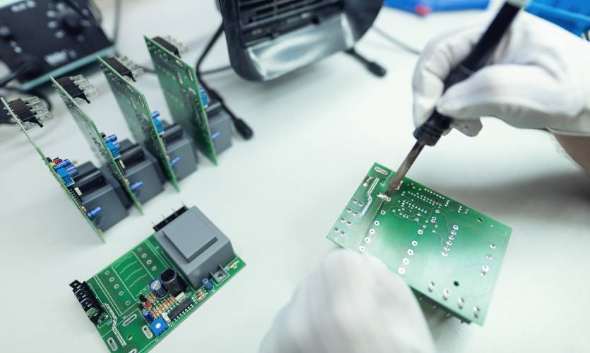
Prototype Manufacturing & Assembly
With the layout finalized, we generate Gerber files and move to fabrication.
- PCBs are fabricated by reliable vendors with specified finishes (HASL, ENIG, etc.)
- Components are assembled either by hand or through SMT machines
- We flash the firmware and test the basic functionality (power-on, I/O test, communication links)
Validation & Field Testing
The prototype is tested under simulated and real-world conditions. We validate:
- Voltage stability and power sequencing
- Temperature tolerance and EMI compliance
- Communication protocols and sensor accuracy
- Compatibility with enclosures and external devices
Documentation & Production Handoff
Once the design is validated, we prepare for production:
- Finalized BOM (Bill of Materials)
- Gerber and drill files
- Assembly drawings and 3D step files
- Test jigs and firmware loaders
- Compliance and certification support (if needed)